I finally managed to unbrick my Chromebook laptop. Here are the gory details in all their redundancy…
These are instructions for
Acer Chromebook 14 CB3-431 (EDGAR)
This is a 1.8V device - Use 1.8V adapter!
Read this first
https://docs.mrchromebox.tech/docs/support/unbricking/unbrick-ch341a.html
For the programmer hardware “stack” I found this page very useful
https://winraid.level1techs.com/t/guide-how-to-use-a-ch341a-spi-programmer-flasher-with-pictures/33041
- Hardware needed
By the time I got my programmer it was no longer available for sale. But there are options.
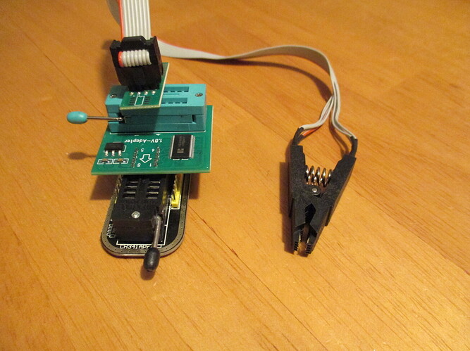
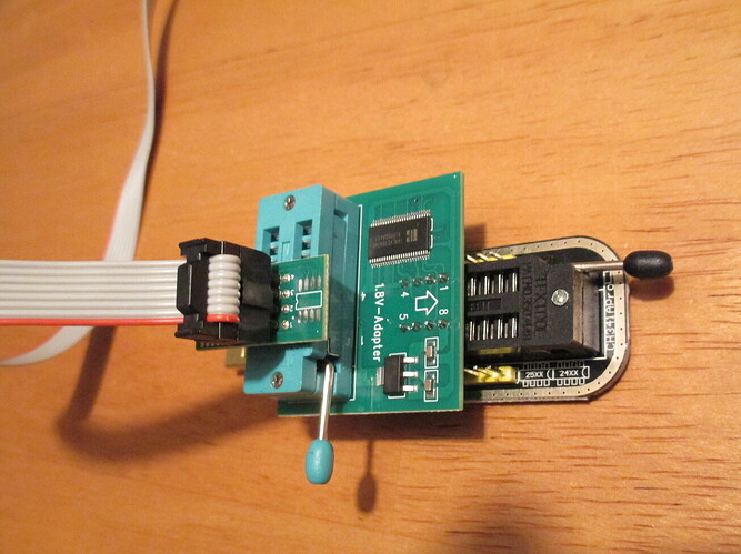
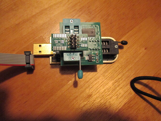
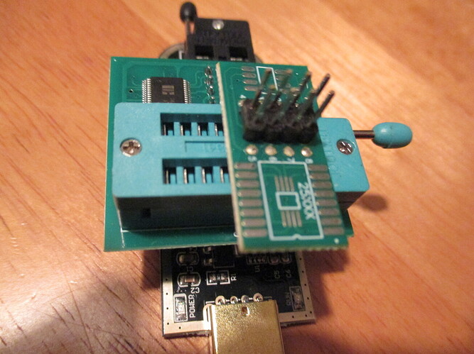
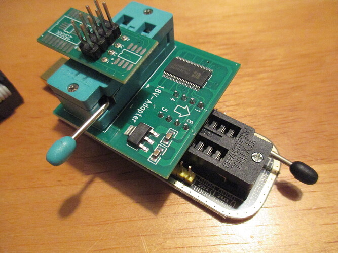
The hardware I used is a CH341a Pro kit which came with a 1.8V adapter, a SOIC8 clip and some other adapters I didn’t use for this unbricking.
The reason I didn’t buy a CH347 is because the programmer alone was more expensive than the kit and it would have taken far longer to arrive.
It may be diffrerent for somebody attempting this at a later date so keep it in mind when shopping for programmers.
There’s also the option of using a pi pico with a level converter which you may already have if you do any embedded electronics as a hobby: then you’d need to buy just the SOIC8 clip.
Tip: Use a light color (e.g. silver) permanent marker to put a dot on the plastic covering pin 1 of the clamp. Red wire in the pictures.
- Linux host machine preparation
Make sure you have the following:
2.1 The BIOS file and its sha1 signature file:
    coreboot_edk2-edgar-mrchromebox_20240914.rom
    coreboot_edk2-edgar-mrchromebox_20240914.rom.sha1
Download using:
wget https://mrchromebox.tech/files/firmware/full_rom/coreboot_edk2-edgar-mrchromebox_20240914.rom
wget https://mrchromebox.tech/files/firmware/full_rom/coreboot_edk2-edgar-mrchromebox_20240914.rom.sha1
Check the file integrity from a terminal:
sha1sum -c coreboot_edk2-edgar-mrchromebox_20240914.rom.sha1
2.2 Make sure the flashrom utility is installed. If not, install with
sudo apt install flashrom
2.3 Optional, if you want to check all the programmer hardware without connecting to a flash chip…
and if you have a DSO scope, connect one channel to the 1V8 adapter pin that would connect to the clock pin of the flash chip (SCLK pin 6) and its ground pin (VSS pin 4).
Use the exposed male header where the SOIC8 clip would go. Confirm the pinout using the datasheet (see below).
To do a single capture, connect the programmer to the host and run in a terminal:
flashrom --programmer ch341a_spi
Since there is no connection to a chip this will fail but the clock line will be active long enough for a capture.
Make sure the output is 1.8 volts by measuring the captured waveform.
I did this before I got time to do the actual disassembly and unbrick because why not?
- Dissassembly and hardware connections
Make sure ESD (electrostatic discharge) precautions are followed!
The procedure required the removal of the motherboard from the machine then flipping of the board to find the flash memory chip to be programmed.
There are some YT videos showing the disassembly of this machine.
Disconnect the battery connector first (and connect it last)!
Remove the WiFi card with both antennas (for BT and WiFi) still attached. Just remove the screw holding it in place and pull it out of the MB.
Once everything is disconnected, remove all screws and then the MB.
Once MB is removed, identify the flash chip and make absolutely sure you got that right before continuing.
The chip to be flashed is near the processor and on its second line has printed 25LQ64CSIG.
It’s a GigaDevices chip in a SOP8 208mil package, so NOT a genuine Winbond chip.
The datasheet I used is 25lq64c.pdf
First, connect the SOIC8 adapter to the flash chip making sure pin 1 is aligned with the dimple on the chip (red wire in pictures).
Make sure the clip has the correct orientation and all pins are making contact.
Plug the CH341a Pro into a USB socket of the host machine.
- Terminal (CLI) commands:
4.1 From the terminal, while in the directory containing the BIOS file run:
flashrom --programmer ch341a_spi
I got the following output:
... some flashrom info ...
Using clock_gettime for delay loops (clk_id: 1, resolution: 1ns).
Found GigaDevice flash chip "GD25LQ64(B)" (8192 kB, SPI) on ch341a_spi.
No operations were specified.
This confirmed I got the proper connection to the flash chip.
4.2 Run the command below to flash the chip.
Make sure the filename is the correct one for your BIOS file!
Only the bios region is written thus saving the boot configuration.
Also note this was run WITH sudo!
sudo flashrom -p ch341a_spi -w coreboot_edk2-edgar-mrchromebox_20240914.rom --ifd -i bios
The output for a successful flash looks like this:
... some flashrom info ...
Using clock_gettime for delay loops (clk_id: 1, resolution: 1ns).
Found GigaDevice flash chip "GD25LQ64(B)" (8192 kB, SPI) on ch341a_spi.
Reading ich descriptor... done.
Using region: "bios".
Reading old flash chip contents... done.
Erasing and writing flash chip... Erase/write done.
Verifying flash... VERIFIED.
- Disconnect the programmer
First remove the programmer from the USB then remove the clip from the chip.
- Reassemble the hardware
Leave the battery connector LAST!
Lift the longest and widest connector (keyboard?) and bend it over the battery (use a piece of tape to stick it out of the way) while reseating the MB. You can’t pull it from under the MB afterwards.
Screw in at least two screws in opposite corners.
Reconnect all the other cables in any order.
Screw in any remaining MB screws.
Check all cables and make sure they are all connected.
Only now reconnect the battery and assemble the back cover.
- Testing (assumes all hardware re-connections are fine)
Plug in a power supply to avoid any potential battery problems.
If both leds are not on (blue and orange), press the power button once and wait. Both leds should be on now (machine on and charging).
If nothing shows on the screen after the time it normally takes after a BIOS update, short press again the power button and the blue led goes out (machine off).
Then after a few seconds short press it again and the blue led should come on (machine on).
After another wait the coreboot logo should come on and the laptop should boot up normally.
- Extra
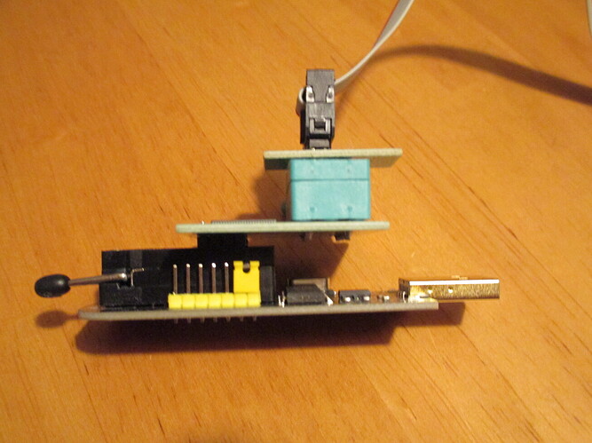
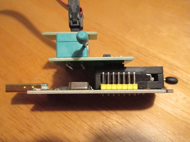
The stack with all the hardware connected as used is illustrated in the pictures.
Note the yellow jumper on the side header: if missing it doesn’t act like a programmer.
Hope this helps someone.
